**PDFs are strictly for personal use only. Copyrights are reserved by respective Publishers!
Please visit my google scholar citations page for full publications.
Selected Publications:

We fabricated a single active layer quantum dot light-emitting diode device based on colloidal CdSe (core)/CdS (arm) tetrapod nanostructures capable of simultaneously producing room temperature electroluminesence (EL) peaks at two spectrally distinct wavelengths, namely, at ∼500 and ∼660 nm. This remarkable dual EL was found to originate from the CdS arms and CdSe core of the tetrapod architecture, which implies that the radiative recombina-tion of injected charge carriers can independently take place at spatially distinct regions of the tetrapod. In contrast, control experiments employing CdSe-core-seeded CdS nanorods showed near-exclusive EL from the CdSe core. Time-resolved spectroscopy measurements on tetrapods revealed the presence of hole traps, which facilitated the localization and subsequent radiative recombination of excitons in the CdS arm regions, whereas excitonic recombination in nanorods took place predominantly within the vicinity of the CdSe core. These observations collectively highlight the role of morphology in the achievement of light emission from the different material components in heterostructured semiconductor nanoparticles, thus showing a way in developing a class of materials which are capable of exhibiting multiwavelength electroluminescence.

Cryptosporidium parvum is a common intestinal parasitic protozoan that causes gastroenteritis in man and animals. It poses high risks to drinking water supply because of its ubiquitous distribution in water and their oocysts are resistant to harsh environment conditions. In this work, we demonstrated the use of large-size chemical vapor deposition (CVD) grown graphene films configured as field-effect device for rapid electrical detection of Cryptosporidium parvum oocysts (Cp. oocysts). The presence of Cp. oocysts causes the change in the transport characteristics of the antibody-functionalized graphene device, which can be measured in terms of the dependence of the drain current on the sweep of the gate voltage or the real-time drain current data under a constant gate voltage. The high sensor sensitivity of 25 oocysts per milliliter solution and good specificity
were evaluated, indicating it a promising candidate for detecting waterborne pathogens in water quality control.
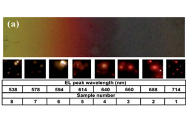
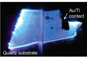
Visible electroluminescence (EL) with tunable wavelength has been observed at room temperature from randomly assembled n-CdSxSe1−xnanowires grown on a p+-SiC substrate by the vapor transport technique. The dominant emission peaks can be tuned from ∼720 to ∼520 nm by varying the composition of the alloy nanowires.

Different distributions of Si nanocrystals (nc-Si) in the gate oxide of Al/nc-Si embedded SiO2/p-SiSiO2/p-Si diodes are synthesized with Si ion implantation technique. Current conduction in the diodes with different nc-Si distributions has been investigated. It is shown that under a positive gate bias Fowler–Nordheim (FN) tunneling from the Si substrate to the oxide, the nanocrystal-assisted conduction (e.g., tunneling,Frenkel–Poole emission) and the nanocrystal-assisted FN tunneling contribute to the current conduction depending on both the nc-Si distribution and magnitude of the gate bias. In the case that nc-Si is densely distributed throughout the oxide, a huge enhancement in the current conduction is observed as a result of the formation of many percolative conduction paths by the nc-Si connecting the gate to the Si substrate.
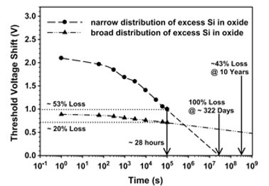
In this work, Si ions are implanted into the gate oxide of MOSFETs with different implantation schemes, followed by a high-temperature annealing. The memory characteristics of the MOSFETs have been investigated for the following two excess Si distributions: (1) the excess Si is distributed in a narrow layer in the gate oxide near the Si substrate; and (2) the excess Si is distributed throughout the gate oxide. It is observed that both the excess Si distributions have good endurance of up to 106 program/erase cycles. The second excess Si distribution exhibits a better retention characteristic with less than 50% charge loss after 10 years. In contrast, the first excess Si distribution shows a complete charge loss after 1 year.
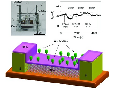
In this paper, we report a label-free sensitive biosensor platform using multi-layer molybdenum disulfide (MoS2) field-effect devices for cancer marker protein detection, which is the first demonstration on the biofunctionalization of MoS2 nanosheet field-effect device and the application of the sensor in liquid-phase. The change in the MoS2 transistor drain current was caused by the specific binding of cancer marker proteins, prostate-specific antigens (PSA), to the anti-bodies that were immobilized onto the MoS2 film surface. From our experimental results, our detection method features high sensitivity and almost instant detection feedback for PSA. In addition to the sub-picomolar sensitivity, the sensor appeared to have good specificity by showing no significant signals to non-target serum protein. This study demonstrates that biofunctionalized MoS2 field effect device is a promising candidate for the detection of cancer markers to advance the early cancer diagnostics.
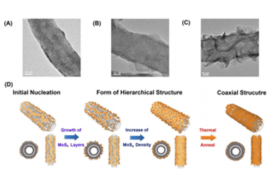
Two dimension (2D) layered molybdenum disulfide (MoS2) has emerged as a promising candidate for the anode material in lithium ion batteries (LIBs). Herein, 2D MoSx (2 ≤ x ≤ 3) nanosheet-coated 1D multiwall carbon nanotubes (MWNTs) nanocomposites with hierarchical architecture were synthesized via a high-throughput solvent thermal method under low temperature at 200°C. The unique hierarchical nanostructures with MWNTs backbone and nanosheets of MoSx have significantly promoted the electrode performance in LIBs. Every single MoSx nanosheet interconnect to MWNTs centers with maximized exposed electrochemical active sites, which significantly enhance ion diffusion efficiency and accommodate volume expansion during the electrochemical reaction. A remarkably high specific capacity (i.e., > 1000 mAh/g) was achieved at the current density of 50 mA g−1, which is much higher than theoretical numbers for either MWNTs or MoS2 along (~372 and ~670 mAh/g, respectively). We anticipate 2D nanosheets/1D WNTs nanocomposites will be promising materials in new generation practical LIBs.

Synthesis, structure, and physical properties of a novel 11-methylbenzo[d]pyreno[4,5-b]furan (BPF) and its self-assembly in water have been reported. The performance of nanowire-based films in organic light-emitting diodes is much better than that of the thin film deposited by directly drop-coating BPF molecules in THF solution. SEM study indicates that the well organized structure (nanowires) is an important factor in enhancing the performance of OLED devices.
Room-temperature random lasing is achieved from an n-AlN/p-GaN heterojunction. The highly disordered n-AlN layer, which was deposited on p-GaN:Mg layer via radio frequency magnetron sputtering, acts as a scattering medium to sustain coherent optical feedback.The p-GaN:Mg layer grown on sapphire provides optical amplification to the scattered light propagating along the heterojunction. Hence, lasing peaks of line width less than 0.4 nm are emerged from the emission spectra at round 370 nm for the heterojunction under forward bias larger than 5.1 V. Lasing characteristics of the heterojunction are in agreement with the behavior of random lasers.
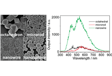
Two novel shapes of 9,10-diphenylanthracene (DPA) micro/nanostructures: octahedron and sphere together with microrod and nanowire have been synthesized via a surfactant-assisted self-assembling process. These micro/nanostructures have been characterized by UVvis, fluorescence spectra, X-ray diffraction (XRD), field emission scanning electron microscope (FESEM), and transmission electron microscope (TEM). Our results indicated that the absorption and emission spectra of as-prepared particles were slightly blue-shift when the shape of DPA particles changed from octahedron to microrod and finally to nanowire. This result could be explained by the different growth directions of DPA micro/nanostructures. To study the relationship between shape and devices’ performance, the heterojunction light emitting diode (LED) devices of quartz/ITO/organic particles/n-SiC/Ti(10 nm)/Au(120 nm) have been prepared. The testing results showed that the different shapes of DPA micro/nanostructures did affect the performance of diodes and the nanowire was the best shape for the heterojunction light emitting diode (LED) devices.
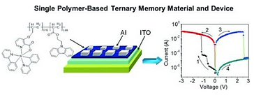
In summary, we have presented the first ternary memory device based on a single polymer with on-chain Ir(III) complexes by combining both the conformational change and CT mechanisms. We have also successfully demonstrated excellent ternary memory performances, including low reading, writing and erasing voltages, and good stability for the three states. Although the detailed mechanism for the ternary memory behaviors need to be further clarified through experimental and theoretical methods, as a proof-of-concept, we hope that the proposed principle combining the multiple memory mechanisms in one polymer system would open up a new and efficient avenue for the design of high-density polymer memory materials and devices. We are now actively pursuing more polymer-based ternary memory materials and devices based on our design principle.
Patents Filed:

-
J. I. Wong, H. Y. Yang, L. Wang, PCT International application no. PCT/SG2013/000463, 2013.

-
J. I. Wong, T. P. Chen, Z. H. Cen and E. S. M. Goh, USA provisional patent application 61/454,886, 2011.

-
T. P. Chen, J. Zhang, J. I. Wong, USA provisional patent application 61/788,540, 2013.